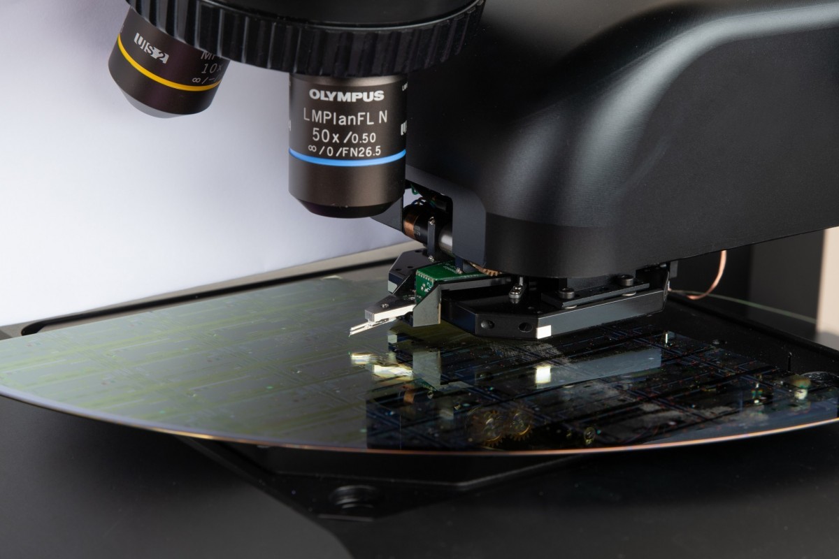
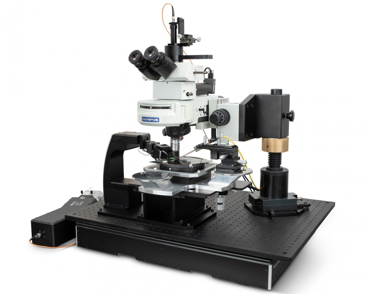
InZiv OmniPix-ML1000 MicroLED Characterization System

MicroLED Characterization System.  Optical and Spectral Information at Unprecedented Resolution

InZiv’s unique technology provides a comprehensive approach to the emerging challenges in microLED defect inspection. A rich set of data coupled with the highest resolution allows display developers and manufacturers to maximize efficiency and yield.


Overview

MicroLED Characterization System

Measure- optical, spectral, and topographical properties of MicroLED pixels and defects

Map– large scale wafers for defective areas

Inspect- pixels, both with photoluminescence (PL) and electroluminescence (EL) on the nm scale

Characterize– optical, spectral, and topographical defects at the submicron scale

Correlate– optical, spectral, and topographical properties of sub-pixel features

Maintain– sample integrity – non-destructive to wafers, display panels, and pixels

InZiv is proud to present the OmniPix-ML1000TM – the first all-encompassing microLED characterization system, offering both full wafer and localized individual pixel inspection. Combining highest resolution optical measurements (both PL and EL) with spectral and topographical data, the OmniPix-ML1000TM provides a state-of-the-art solution for microLED inspection and characterization.

The OmniPix-ML1000TM integrates multiple inspection modalities in one system, and provides an unprecedented, comprehensive analysis of the pixel features. The OmniPix-ML1000TM empowers microLED developers with the ability to better understand the relationship between light, color, and structure – directly addressing some of today’s most critical challenges in microLED. 

With pixels currently being developed on a scale as small as single-microns, only the highest resolution techniques can meet today’s most rigorous characterization demands. The OmniPix-ML1000 enables accurate optical and spectral characterization of individual defective, dim, and dead pixels. Using one system, you can identify irregularities in color, brightness, and structure in the microLED wafer, while subsequently examining the most problematic pixel features at the highest resolution.

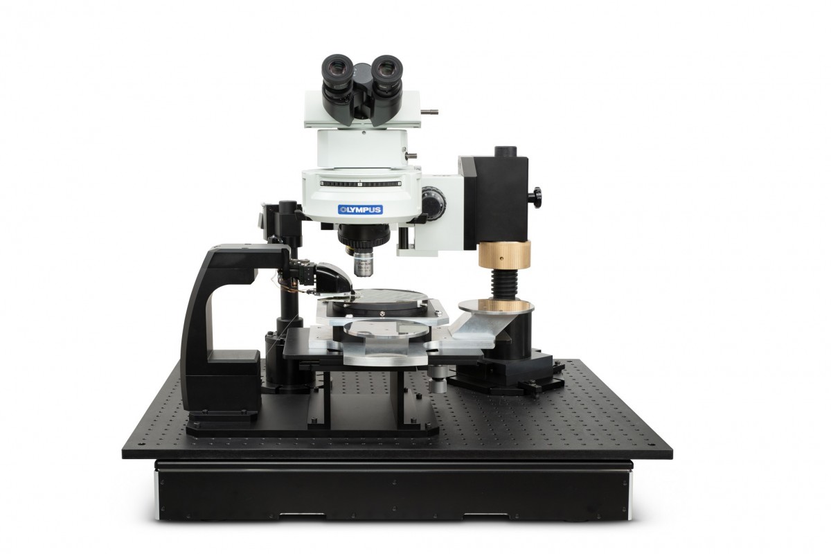
 

Specifications

Optical lateral resolution (XY) 100 nm
3D Measurements XY <10nm
Z <0.5nm
Hyper-spectral imaging – correlated with 3D structure 1 nm
Sample scanning Up to 100 µm in X,Y 20µm in Z
Tip scanning Up to 35 µm in X,Y,Z
Scanner resolution Z<.005 nm
XY<0.015 nm (standard)
XY<0.002 nm (low voltage mode)
Noise characteristics <0.2 nm p-p
<0.07 nm RMS
PL excitation source Laser with suitable wavelength as per customer need
PL resolution 100nm
Spectral resolution 1 nm
Spectral range 350nm-800nm

Luminesence

  • Reflection
  • Photoluminescence/nano-PL with spatial resolution of <100 nm
  • Electroluminescence/micro-EL
  • Dead or dim pixels
  • Luminescence non-uniformities with spatial resolution of <100 nm
  • Output light efficiency
  • Light extraction efficiency
  • Low external quantum efficiency (EQE)
  • Beam shaping
  • Optical crosstalk
  • Time-resolution refresh times with ns resolution

Spectral

  • Wavelength non-uniformities with spatial resolution of <100nm
  • Spectral variations within the pixel, correlated with defect type

Electrical

  • Conductivity
  • Energy transfer
  • Voltage non-uniformities

Material

  • Material non-uniformities at high resolution
  • Foreign material detection and identification

Thermal

  • Thermal non-uniformities
  • Thermal instability

Structural

  • Pits, scratches, dust particles
  • Displaced pixels
  • Sidewall defects
  • Structural irregularities
  • 3D images of defects

Request Info / Demo